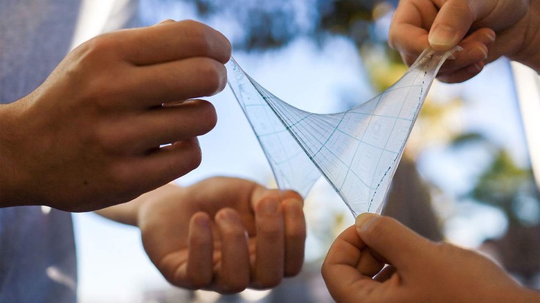
Stanford Researchers Create Stretchable Circuits That Flex With The Body
A group of researchers from Stanford have spent the last two decades working to develop skin-like integrated circuits that can be stretched, folded, bent, twisted without damaging their operating capability. The stretchable circuits can return to their original shape every time they are stretched. One major hurdle that has been in the way of the research is determining how to produce the new technology in large enough quantities for commercialization.The group has published a new study describing how they printed stretchable and durable integrated circuits on rubbery skin-like materials using the same type of equipment that builds solid silicon chips. The breakthrough could allow the new material to be easily commercialized by changing foundries that are currently making rigid circuits to factories that produce flexible ones. The researchers were able to squeeze more than 40,000 transistors into a single square centimeter of stretchable circuitry.
Researchers on the project believe they will double the number of transistors on a square centimeter soon. However, they admit that the number of transistors that can print on their flexible material is very far away from the billions of transistors that can be printed onto silicon of the same size. However, their flexible material would contain enough transistors to create simple circuits for functions such as on-skin sensors, body-scale networks, implantable by electronics, and possibly more.
The breakthrough construction method improves the elastic-transistor destiny by more than 100 times what anyone else has been able to achieve while maintaining excellent uniformity in transistors. The material also sacrifices nothing in electronic or mechanical performance to gain its flexibility.
The big gain for the process invented by Stanford is that their flexible circuits can be created using equipment that's already inside foundries. The building process is known as photolithography and uses ultraviolet lights to transfer a detailed electrically active geometric pattern onto a solid substrate layer by layer. The team also notes their processes more cost-effective and may enable stretchable circuits to be produced at less cost than rigid ones.
